How to Choose the Right Test Probes for Accurate Functional Testing of SMT PCBsAuthor : Adrian September 12,pasta de solda caseiro 2025Table of ContentsChoosing the right test probes for functional testing of Surface Mount Technology (SMT) Printed Circuit Boards (PCBs) is crucial for ensuring accurate results and maintaining the quality of your electronic assemblies. With the increasing complexity of SMT designs, selecting the appropriate tools, such as SMT test probes, can make or break the testing process. Factors like PCB test probe selection, fine pitch probe compatibility, test probe resistance, PCB test point size, and probe maintenance all play a significant role. In this comprehensive guide, we’ll walk you through the essentials of selecting the best test probes for your needs, providing actionable insights and practical tips to achieve reliable testing outcomes.
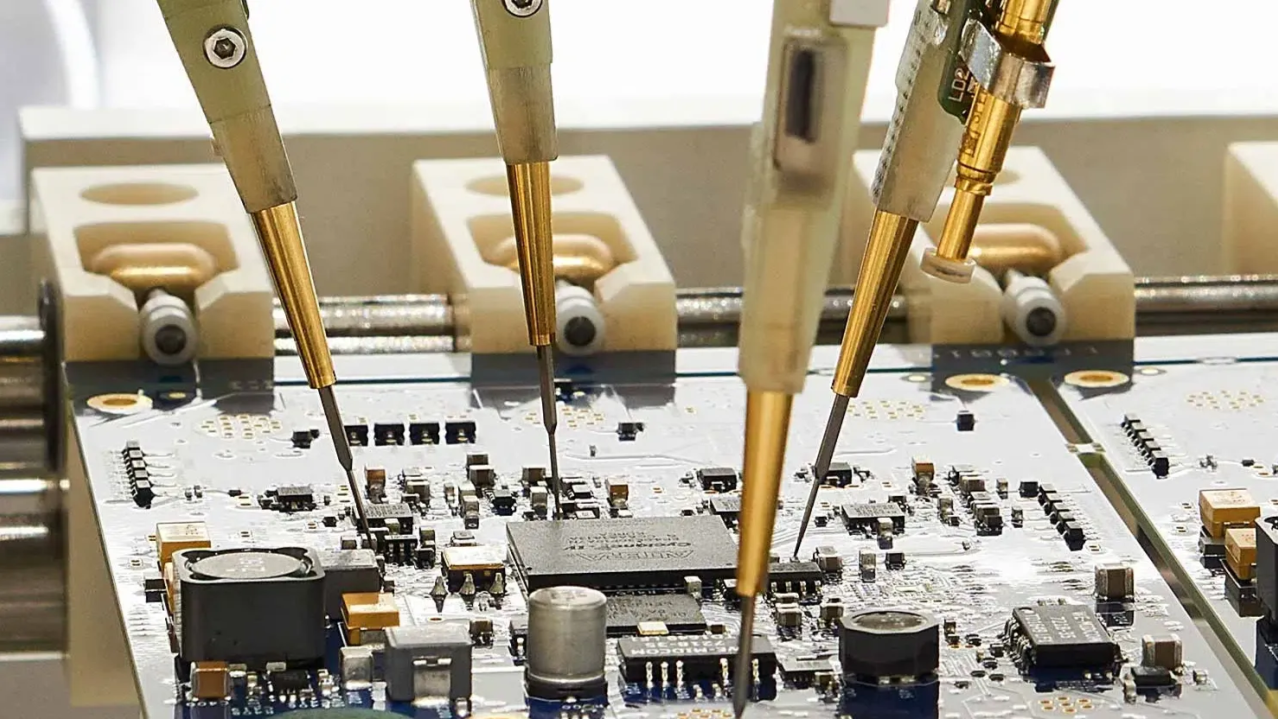
Why Test Probes Matter in SMT PCB Functional TestingFunctional testing of SMT PCBs ensures that the assembled board performs as intended under real-world conditions. Test probes are the critical link between the test equipment and the PCB, making direct contact with test points to measure electrical signals, continuity, and functionality. A poor choice of probes can lead to inaccurate readings, damaged components, or even complete test failures. By focusing on proper PCB test probe selection, you can avoid these pitfalls and ensure consistent, reliable results. In SMT designs, components are smaller and more densely packed than in traditional through-hole technology. This means test points are often tiny and closely spaced, requiring precision tools like fine pitch probes. Understanding the nuances of probe selection and maintenance is key to tackling these challenges effectively.
Key Factors in PCB Test Probe SelectionSelecting the right test probes for SMT PCBs involves evaluating several critical factors. Let’s break down each one to help you make an informed decision. 1. Compatibility with PCB Test Point SizeOne of the first considerations in PCB test probe selection is the size of the test points on your board. SMT PCBs often feature test points as small as 0.5 mm or less in diameter, especially in high-density designs. Using a probe that is too large can result in poor contact, misalignment, or damage to the test point and surrounding components. To match the probe to the PCB test point size, check the specifications of your board’s design files. For instance, if your test points are 0.8 mm, opt for a probe tip with a diameter slightly smaller or equal to ensure a secure connection without excessive force. Probes with spring-loaded tips can also help by providing consistent pressure without damaging delicate pads.
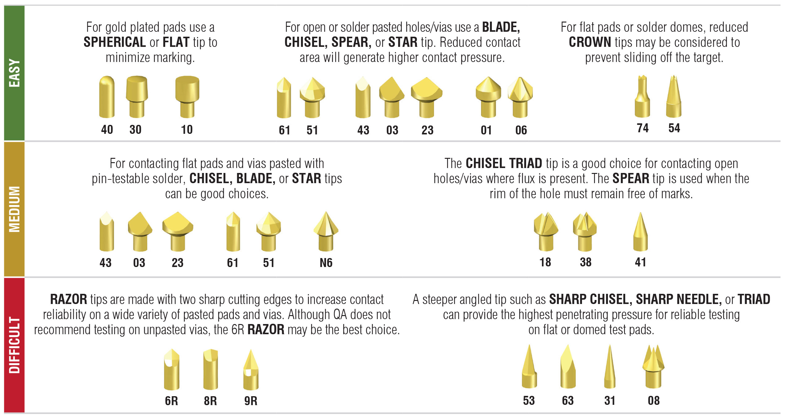
2. Fine Pitch Probe Requirements for High-Density BoardsAs SMT technology advances, components are placed closer together, often requiring fine pitch probes for testing. Fine pitch refers to the small spacing between test points or component leads, sometimes as narrow as 0.2 mm. Standard probes may struggle to access these areas without causing short circuits or missing the target entirely. Fine pitch probes are designed with ultra-thin tips to navigate tight spaces. When selecting these probes, consider the pitch of your PCB layout. For example, a board with a 0.5 mm pitch will need a probe tip diameter of 0.3 mm or less to avoid interference with adjacent points. Additionally, ensure the probe material and design can handle repeated use without bending or breaking in such precise applications. 3. Understanding Test Probe Resistance for Accurate MeasurementsTest probe resistance is another critical factor that affects the accuracy of functional testing. Resistance in the probe tip or contact point can introduce errors in voltage or current measurements, leading to false positives or negatives in your test results. Ideally, you want probes with low contact resistance, typically below 50 milliohms, to minimize signal loss. For SMT PCBs, where signals are often low-voltage and high-frequency, even small resistance variations can skew results. Look for probes made from high-conductivity materials like gold-plated beryllium copper, which offer excellent conductivity and durability. Regularly testing and calibrating your probes can also help detect any increase in resistance over time due to wear or contamination. 4. Probe Tip Style and Shape for Specific ApplicationsThe shape and style of the probe tip can significantly impact its effectiveness during testing. Different SMT PCB designs may require specific tip styles to ensure proper contact and avoid damage. Common tip styles include:
Choose the tip style based on the surface characteristics of your PCB and the nature of the test points. For instance, if your board has flat, smooth pads, a cupped tip might be the best choice to prevent slipping during testing.
5. Durability and Material QualityTest probes endure significant wear and tear during repeated testing cycles. Choosing probes made from durable materials ensures longevity and consistent performance. Probes with stainless steel bodies and gold-plated tips are popular for their resistance to corrosion and excellent conductivity. Additionally, spring-loaded probes should have robust internal mechanisms to maintain consistent contact pressure over thousands of cycles. For high-volume testing environments, investing in high-quality probes can save costs in the long run by reducing the need for frequent replacements. Check manufacturer specifications for cycle life ratings, which indicate how many test cycles a probe can handle before performance degrades—some premium probes can exceed 100,000 cycles.
Probe Maintenance: Extending the Life of Your SMT Test ProbesEven the best test probes will underperform if not properly maintained. Probe maintenance is essential to ensure consistent accuracy and prevent damage to both the probes and the PCBs being tested. Here are some practical tips to keep your SMT test probes in top condition. 1. Regular Cleaning to Prevent ContaminationOver time, test probes can accumulate dirt, flux residue, or oxidation on their tips, increasing contact resistance and leading to unreliable measurements. Clean your probes after every testing session using a soft cloth or brush and a mild solvent like isopropyl alcohol. Avoid abrasive materials that could scratch the tip surface, especially on gold-plated probes. For stubborn residues, use a specialized probe cleaning tool or pad designed for delicate electronics. Regular cleaning not only improves accuracy but also prevents contamination from transferring to the PCB, which could cause shorts or other issues. 2. Proper Storage to Avoid DamageImproper storage can bend or damage probe tips, especially for fine pitch probes with ultra-thin designs. Store your probes in a protective case or holder when not in use, ensuring the tips are not under pressure or in contact with other objects. Avoid stacking heavy items on top of stored probes, as this can deform the spring mechanisms or tips. 3. Routine Inspection for Wear and TearInspect your probes regularly for signs of wear, such as bent tips, worn plating, or reduced spring tension. A damaged probe can cause inconsistent contact or even scratch the PCB surface, leading to costly repairs. If you notice any issues, replace the probe immediately to avoid compromising test accuracy. Keeping a log of usage cycles can help predict when a probe might need replacement based on its rated lifespan.
Testing Methods and Probe CompatibilityDifferent functional testing methods for SMT PCBs may require specific types of probes. Understanding the testing approach you’ll use can guide your probe selection. Here are a few common methods and their probe requirements:
Ensure your probes are compatible with the testing equipment and method you’re using. For instance, flying probe systems often have specific probe holders or connectors, so check the system specifications before purchasing.
Practical Tips for Choosing SMT Test ProbesHere are some actionable tips to simplify the process of selecting and using test probes for SMT PCB testing:
Conclusion: Making the Right Choice for Reliable SMT PCB TestingChoosing the right test probes for functional testing of SMT PCBs is a multi-faceted process that requires attention to detail and an understanding of your specific testing needs. By focusing on key factors like PCB test point size, fine pitch probe compatibility, test probe resistance, and proper probe maintenance, you can ensure accurate and reliable results every time. High-quality probes, paired with consistent care and the right testing methods, will help you maintain the integrity of your SMT assemblies and deliver top-notch electronic products. At ALLPCB, we understand the importance of precision in every step of PCB manufacturing and testing. Whether you’re dealing with high-density SMT designs or complex functional testing requirements, selecting the right tools is essential. Use this guide as a roadmap to make informed decisions about SMT test probes and elevate the quality of your testing process. Share · · · · The Role of Flux in PCB Wave Soldering: Selection, Application, and Residue RemovalMarch 16, 2026PCB wave soldering flux types include rosin, water-soluble, and no-clean options with varying activity levels for oxide removal and solder flow. This guide covers selection criteria, spray foam drop-jet application methods, residue removal processes, and alternatives like nitrogen blanketing to boost joint reliability and yields for engineers. Article Achieving Uniform Solder Fillets in PCB Wave Soldering: Process ControlMarch 16, 2026Achieve uniform solder fillets in PCB wave soldering with process control strategies. Optimize flux, preheat, wave height, conveyor speed for consistent fillet shape, height, and wetting balance. Includes visual inspection tips and troubleshooting for reliable through-hole assemblies. Boost quality in production. Article Optimizing Conveyor Speed for Efficient PCB Wave SolderingMarch 16, 2026Learn PCB wave soldering conveyor speed calculation to manage dwell time, immersion depth, and throughput effectively. Electric engineers get practical steps, best practices, and troubleshooting tips for higher process efficiency and fewer defects in wave soldering operations. Article Understanding IPC Standards for PCB Surface Finishes: Ensuring Quality and ComplianceMarch 11, 2026Understand IPC standards IPC 4552 ENIG and IPC 4553 immersion silver for PCB surface finishes. Ensure compliance, enhance solderability, and prevent common defects to achieve reliable, high quality circuit boards. Article High Speed Routing Techniques: PCBMarch 11, 2026Master high speed routing in PCBs to ensure signal integrity and minimize electromagnetic interference. Learn essential techniques for robust designs, from controlled impedance to differential pair strategies. Prevent performance issues and achieve reliable electronics. Article Miniaturization Challenges in PCB AssemblyMarch 11, 2026Navigate the complexities of high density interconnect PCB assembly and precise component placement. Learn to tackle miniaturization challenges, from tiny part handling to thermal stress, ensuring robust and reliable electronics. ArticleGet Instant PCB |